Introduction
Demand for high-gain, low-profile antenna systems is accelerating across defense, satellite communications, aviation, and maritime sectors. According to Strategic Market Research, the phased-array antenna market is projected to grow from $3.1B in 2024 to $5.3B by 2030 at a 9.4% CAGR, with defense and radar applications representing approximately 42% of that demand.
Patch antenna arrays are driving much of that growth. They're low-profile, PCB-compatible, and scalable — a practical choice for programs that need directional gain without the bulk of traditional antenna structures.
This guide walks through the complete design process:
- Single patch element design and substrate selection
- Feed network architecture and array layout
- Full-array simulation and performance analysis
- Prototyping, testing, and moving toward production
Whether you're an RF engineer working a defense program or a systems integrator evaluating patch array technology for production, each section covers the decisions that matter at that stage of development.
Key Takeaways
- A single patch element produces roughly 6–9 dBi of gain; a 4×4 array can exceed 14 dBi in simulation
- Substrate choice drives efficiency, bandwidth, and patch size — Rogers/PTFE laminates offer lower loss tangent than FR4, making them the correct choice for microwave-frequency designs
- Corporate feeds with Wilkinson dividers deliver uniform excitation across planar arrays — the standard topology for controlled aperture distribution
- Near-field chamber testing gives the most accurate gain and pattern data — outdoor far-field approximations introduce avoidable error
- Production-ready designs demand material traceability, environmental qualification, and AS9100 compliance — not just electrical performance
What Is a Patch Antenna Array? Fundamentals and Key Concepts
The Single Patch Element
A patch antenna (microstrip antenna) is a metallic patch — typically rectangular — bonded to a dielectric substrate over a ground plane. The patch resonates when its length is approximately half a wavelength at the target frequency. Radiation doesn't come from the patch surface itself; it comes from the fringing fields at the radiating edges, where the electric field extends beyond the patch boundary into free space.
This distinguishes patch antennas from waveguide radiators and dipoles, which radiate through fundamentally different mechanisms.
The result is a compact, flat radiator that can be fabricated directly on PCB substrates — a direct fit for aircraft fuselages, maritime housings, and satellite terminals where space and aerodynamics constrain antenna options.
Why Arrays?
A single patch element typically produces roughly 6–8 dBi of directivity, with conventional designs reaching 8–9 dBi of gain in practice. That's adequate for some short-range applications, but insufficient for satellite uplinks, phased array radar, or GNSS where high directivity is non-negotiable.
Combining multiple elements into an array multiplies directivity. Published results illustrate the gain levels arrays can reach:
- A 4×4 circularly polarized array for small-satellite data transmission achieved 15.5 dBic peak gain
- A dual-polarized 39 GHz 4×4 array for aviation cabin connectivity reached approximately 18 dBi simulated gain
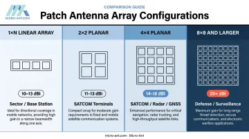
Common Array Configurations
| Configuration | Typical Use Case | Gain Range |
|---|---|---|
| 1×N linear array | Sector coverage, base stations | 10–13 dBi |
| 2×2 planar | Moderate-gain SATCOM terminals | 11–13 dBi |
| 4×4 planar | High-gain SATCOM, radar, GNSS | 14–18 dBi |
| 8×8 and larger | High-directivity defense/surveillance | 20+ dBi |
Inherent Trade-Offs
Patch arrays aren't without limitations. Understanding these trade-offs before committing to a design avoids costly iteration:
- Standard microstrip-fed patches are typically under 5% bandwidth; most designs land around 1–3%
- Every power division stage in the feed network introduces insertion loss, degrading realized gain below simulated directivity
- Thicker substrates improve bandwidth but increase surface wave losses across the array aperture
Key Design Parameters for a Single Patch Element
Patch Dimensions: Width and Length
Two primary dimensions define a rectangular patch: width (W) and length (L).
Width is calculated first, using the free-space velocity of light and the average of the substrate's relative permittivity (εr) and air (εr = 1). A wider patch improves radiation efficiency and reduces input impedance at the radiating edge.
Length requires an additional step. Because fringing fields make the patch electrically longer than its physical dimension, an effective permittivity (εreff) is computed (accounting for the ratio of substrate height to patch width) and then applied to calculate the corrected resonant length.
That corrected length includes a fringe effect compensation term (ΔL). An error in patch length shifts the resonant frequency proportionally, making accurate ΔL compensation non-negotiable.
Substrate Selection
Substrate choice affects efficiency, bandwidth, patch size, and fabrication cost. The core trade-off:
- Low-εr substrates (Rogers RT/duroid 5880: Dk 2.20 ±0.02; RO4003C: Dk 3.38 ±0.05): Higher efficiency, wider bandwidth, larger physical patch size. Preferred for professional defense and SATCOM programs
- Higher-εr substrates (FR4-class materials): Inexpensive and PCB-compatible, but Dk varies significantly by glass/resin construction and frequency (approximately 4.10–4.60 at 1 GHz for Isola IS420). Higher loss tangent reduces efficiency. Acceptable for prototyping at lower frequencies
- Substrate thickness: Thicker substrates improve bandwidth but introduce surface wave modes that couple energy between elements and degrade array pattern — a genuine concern in arrays beyond a few elements
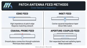
Feed Method Options
Impedance matching at the feed point is where many first designs fail. The main options:
- Edge feed: High impedance at the radiating edge (roughly 150–300Ω for typical patches, varying with geometry). Requires an external matching network
- Inset feed: The feed point moves inward along the patch. Input resistance follows a cosine-squared taper: Rin(y₀) = Rin(0) × cos²(πy₀/L). Moving the feed inward reduces impedance ; select inset depth y₀ to reach 50Ω directly
- Coaxial probe feed: Connects from the ground plane through the substrate. Useful when microstrip feed lines would introduce unwanted radiation
- Aperture-coupled feed: Separates the feed network from the radiating element with a slot in the ground plane. Adds complexity but enables wider bandwidth and better isolation between feed and radiator
Ground Plane Sizing
A commonly overlooked detail: the ground plane must extend sufficiently beyond the patch perimeter to prevent edge diffraction from distorting the radiation pattern. Design guidelines recommend extending it by approximately 6× the substrate height (h) on each side.
Undersized ground planes shift the resonant frequency and break pattern symmetry — a frequent cause of prototype failures that don't match simulation.
Specialized Element Configurations
For circular polarization applications (GNSS, SATCOM uplinks), two approaches dominate:
- Truncated-corner patches: Removing small triangular sections at opposing patch corners splits the degenerate modes into orthogonal modes with 90° phase separation, producing RHCP. A GPS L5 example using this method reported 6.1 dBi peak gain with 1.02% axial-ratio bandwidth
- Dual-feed patches: Two feed points with a 90° hybrid coupler provide more bandwidth and better axial ratio than truncated corners, at the cost of added network complexity
Designing the Feed Network and Array Layout
Corporate vs. Series Feed
The feed topology determines how signal reaches each radiating element. The two main options — series and corporate — involve a direct tradeoff between compactness and phase stability.
Series feed connects elements in a chain along a single transmission line. It's compact, with lower insertion loss from shorter feed lines. The tradeoff: the phase relationship between elements is frequency-sensitive. Beam squint and uneven power distribution limit its usefulness for most planar array applications.
Corporate (parallel) feed routes signal from a single input through cascaded power dividers to reach all elements simultaneously. Key characteristics:
- Equal electrical path lengths ensure in-phase excitation across the array
- Maintains consistent gain and performance over a wider bandwidth
- Longer feed lines increase insertion loss compared to series feed — an acceptable tradeoff for most planar array designs
For arrays requiring uniform excitation and predictable beam behavior, corporate feed is the standard choice.
Wilkinson Power Dividers
With the feed topology selected, the next design decision is the splitting element. The Wilkinson divider is the standard choice for corporate feed networks. For a 50Ω system:
- Quarter-wavelength arms: 70.7Ω (= √2 × 50Ω)
- Isolation resistor between output ports: 100Ω (= 2 × 50Ω)
All three ports present matched impedances, minimizing inter-port reflections. Line widths for the 70.7Ω arms are calculated from the substrate parameters — narrower than the 50Ω feed lines, so leave room in your layout for the width transitions.
Element Spacing
Half-wavelength (0.5λ) center-to-center spacing is the standard starting point. It satisfies the spatial sampling condition that prevents grating lobes from appearing in the visible region for broadside radiation.
Spacing beyond 0.5λ increases the effective aperture for a fixed element count, which can improve directivity. The risk: grating lobes appear when the array is scanned off broadside. For a scanning array, the safe maximum spacing is governed by the scan angle:
d_max < λ / (1 + |sin θ_max|)
Validate spacing selection in simulation across your intended scan range before committing to a layout.
Path Length Matching
Every feed trace from the input port to each radiating element must be equal in electrical length. Unequal path lengths introduce phase errors that reduce gain and tilt the beam off the intended direction.
When the physical layout makes equal-length traces difficult — in larger arrays especially — meandering traces add electrical length without enlarging the board footprint. These deliberately routed squiggly sections are standard practice for array feed routing.
Simulating and Analyzing Patch Antenna Array Performance
Simulation Workflow
Start with a single-element simulation before building the full array. Common EM solvers — tools like Ansys HFSS (FEM-based), CST Studio Suite, and Altair Feko (Method of Moments) all support this staged workflow.
Single-element validation checklist:
- Define the substrate stackup accurately: metal thickness, conductor material (copper), substrate height, and εr at the target frequency
- Set the frequency plan to sweep through and above the target resonant frequency
- Use sufficient mesh density to resolve fine features — especially the inset gap, where under-meshing causes inaccurate impedance results
- Confirm S(1,1) minimum aligns with the target frequency and the Smith chart impedance crosses the real axis at 50Ω
Only after single-element results match expectations should you build the full-array model.
Key Simulation Outputs
At each stage, validate these outputs before proceeding:
| Output | What to Check |
|---|---|
| S(1,1) return loss | Minimum at target frequency; typically < –10 dB |
| Smith chart | Real-axis crossing at 50Ω at resonance |
| 3D far-field pattern | Symmetric main beam, acceptable side lobe levels |
| Gain | Compared against element count and expected array factor |
| Directivity | Higher than gain — the difference reflects total losses |
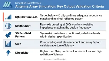
Gain vs. directivity: Directivity measures how focused radiated power is geometrically, ignoring losses. Gain accounts for real efficiency losses: feed network insertion loss and substrate dissipation.
For a corporate-fed 4×4 array, the gap between simulated directivity and realized gain typically runs 2–4 dB depending on substrate and feed network design. This is expected, not a sign of an error.
Common Simulation Pitfalls
- Wrong patch length: Shifts resonant frequency proportionally. Double-check dimensional inputs before running
- Inset gap capacitance: Can cause the S(1,1) minimum and Smith chart real-frequency crossing to occur at slightly different frequencies — this is a real physical effect, not a simulation error
- Insufficient mesh density: Fine features like inset gaps and Wilkinson resistors require finer mesh than the default settings provide
- Single simulation isn't enough: Expect multiple iterations with parameter sweeps. This is normal engineering, not a sign of a flawed approach
Prototyping and Testing Your Patch Antenna Array
PCB Fabrication Considerations
Select a PCB manufacturer whose actual substrate material matches your simulation assumptions — specifically εr, substrate height, and copper thickness. Fabrication tolerances introduce real frequency shifts. One published example at 77 GHz on Rogers RO3003 measured a 2.5–3 GHz upward frequency shift because the actual Dk at W-band was approximately 2.8 rather than the datasheet value of 3.0.
Practical fabrication notes:
- Etching can round corners by 2–5 mil, which matters at higher frequencies
- ±0.5 mil tolerance on a 4–5 mil conductor is roughly 20% geometry variation at mmWave
- Ensure the ground plane extends sufficiently beyond the array edge per your design spec
- Define the SMA connector mounting point and footprint in your fabrication files — connector parasitics affect resonant frequency and return loss
Expect the first prototype to require tuning. That's not a failure; it's a data point.
Testing Approaches
Basic electrical verification: A VNA measurement of S(1,1) confirms resonant frequency and return loss. This is the minimum first step — quick to execute and immediately tells you whether the prototype is in the right frequency neighborhood.
Far-field gain measurement: Outdoor substitution measurements are possible if the far-field condition is met: distance ≥ 2D²/λ from the antenna aperture (where D is the largest aperture dimension). This becomes impractical as antenna size or frequency increases.
Near-field chamber testing: Planar and spherical near-field scanning provide the most accurate, repeatable gain and radiation pattern data without requiring large outdoor ranges. Spherical scanning captures radiation over all angles; planar scanning is well-suited to directive antennas.
Micro-Ant's Jacksonville, Florida facility operates both spherical and planar near-field chambers covering 750 MHz to 40 GHz, which spans the full range relevant to patch array programs from L-band GNSS through Ka-band SATCOM.
Expected Prototype Performance
A 4×4 patch array designed for 2.45 GHz on FR4 can achieve 12–15 dBi in simulation, depending on feed network efficiency and element spacing. One published IEEE result for a 4×4 FR4 square patch array reported 12.15 dBi simulated and 12.08 dBi measured, a difference of less than 0.1 dBi. Real-world performance depends on your specific substrate, feed network design, and fabrication quality — calibrate expectations against your actual design, not published averages.

From Prototype to Production-Ready Design
A working prototype proves the concept — but production-ready hardware carries a different set of requirements that go well beyond electrical performance:
- Manufacturing tolerances: Design rules must accommodate the εr and dimensional tolerances of production substrates, not just the nominal simulation values
- Environmental qualification: Defense and aerospace programs require vibration, thermal cycling, and humidity testing — typically per MIL-STD-810H — to demonstrate performance under life-cycle stresses
- Material traceability: AS9100:2016 adds aviation, space, and defense requirements on top of ISO 9001:2015's quality management framework — covering material documentation and configuration management throughout production
- Repeatability: A design that works in prototype quantities must be manufacturable consistently at production volumes
For organizations whose core competency isn't antenna engineering, this transition is where programs most often stall. Micro-Ant has spent over 20 years navigating this gap, taking programs from concept through tested, production-qualified hardware across defense, SATCOM, and aviation applications. AS9100:2016 and ISO 9001:2015 certified with production capacity exceeding 200,000 units per year, Micro-Ant handles custom substrate selection, feed network optimization, near-field characterization, and environmental qualification — all under one roof in Jacksonville, Florida.
Frequently Asked Questions
What is a patch array antenna?
A patch array antenna is a group of individual patch (microstrip) antenna elements arranged on a shared substrate and connected through a common feed network. Working together, they produce higher gain and directivity than any single element could achieve alone.
How does an antenna array work?
Multiple radiating elements are fed simultaneously through a network that controls the phase and amplitude reaching each element. When elements are fed in phase with proper spacing, their signals add constructively in the intended direction, increasing gain and narrowing the beam.
What are the advantages and disadvantages of patch antenna arrays?
Key advantages include low profile, PCB compatibility, scalable gain, and the ability to conform to curved surfaces. Disadvantages include narrow bandwidth (typically 1–5%), feed network losses that reduce realized gain, and greater design complexity compared to a single-element radiator.
What substrate material is best for designing a patch antenna?
Low-εr, low-loss laminates like Rogers RT/duroid 5880 (Dk 2.20) or RO4003C (Dk 3.38) deliver the best efficiency and bandwidth for high-performance applications. FR4-class materials are cost-effective for prototyping at lower frequencies where their higher and variable loss tangent is an acceptable trade-off.
What is the difference between corporate feed and series feed in an antenna array?
Corporate feed connects all elements in parallel through cascaded power dividers, ensuring equal path lengths and in-phase excitation, which produces better bandwidth and uniform gain. Series feed connects elements in series along a single transmission line, which is simpler but more frequency-sensitive and prone to beam squint and uneven power distribution.
How much gain can a patch antenna array achieve?
A single patch element typically produces 6–9 dBi. A 4×4 array can achieve 14–18 dBi in simulation depending on frequency, substrate, and feed network design. Larger arrays push gain higher, though feed network insertion losses increasingly limit realized gain as element count grows.